In this article, we will have a brief overview of GPU Hardware from programming perspective. I am a software engineer and I do not have time or resources to learn nitty-gritty details of hardware engineering. However, learning about hardware is essential to write efficient and clean programs. I have learned it hard way during my stint at Samsung. We will be looking at discrete GPU setup, then understand how modern NVIDIA GPUs look like and then try to understand each part (from NVIDIA whitepaper)
Discrete GPU Setup
Discrete GPU setup is where we have GPU Hardware that is coupled away from CPU and communicate with CPU using PCIe/NVLink connections and driver code. The other kind would be integrated GPU, where GPU silicon which is part of SoC and shares memory with CPU. The figure below is a typical CPU-GPU Setup.
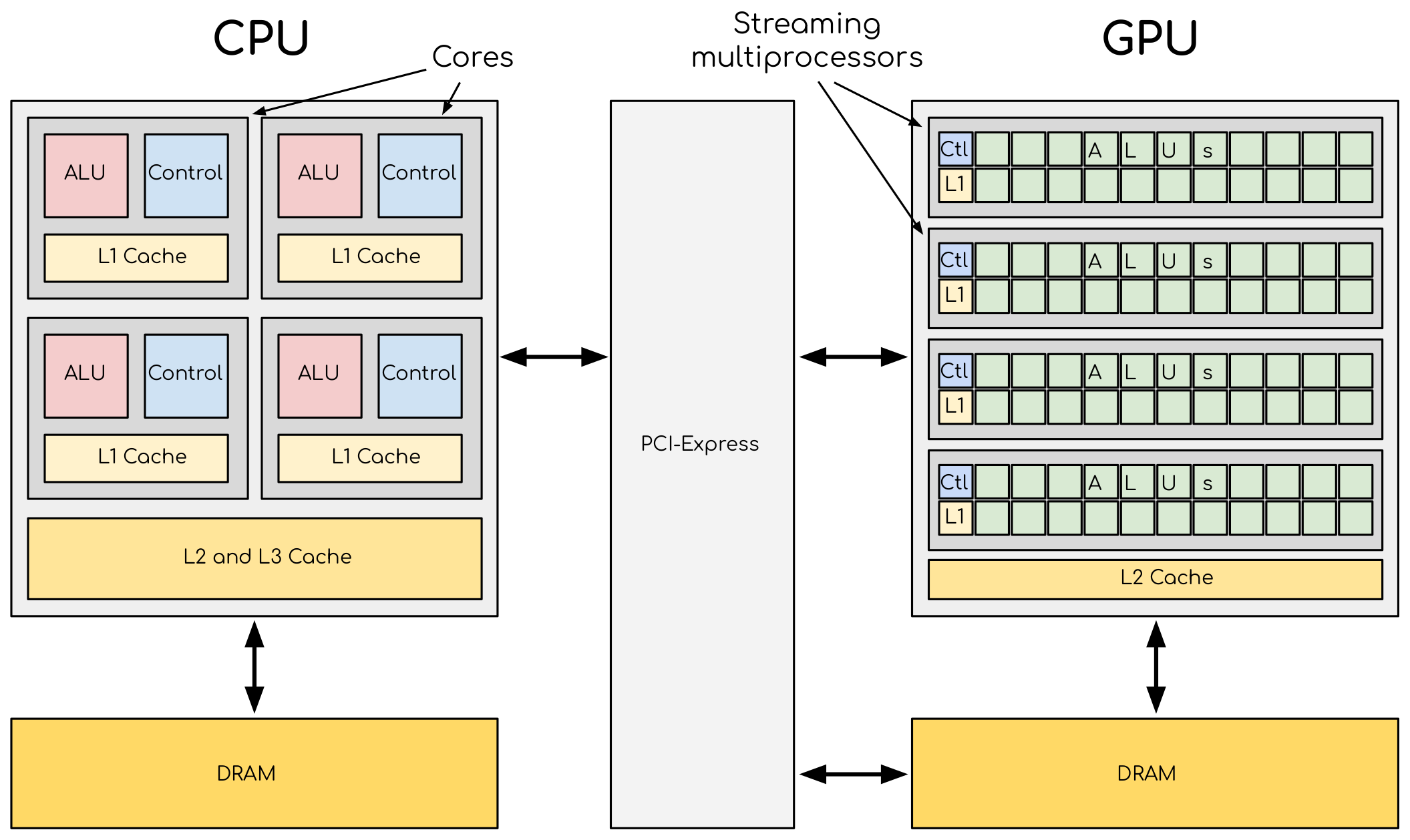
Structure of a typical CPU-GPU Setup. source: here
Before starting comparison, let us see what is PCI-Express ? Peripheral Component Interconnect Express is a type of hardware connection that enables high speed data transfer between two components. It is a standard based on current technological needs and technology (similar to USB Type C), and hardware people can have simple time designing for connection.
Let us notice few differences between CPU and GPU:
- Size each ALUs in GPU is smaller compared to CPU.
- Smaller Cache and Control Unit sizes in GPUs compared to CPU.
- Number of ALUs in GPU is way bigger compared to CPU.
- DRAM is different in CPU and GPU.
All these difference are due to trade-off decision taken by GPU Hardware engineer to deliver maximum floating point operations per second. So, CPUs have lot of features like:
- hardware hyper-threading enabling speculative execution to deliver absolute speed in sequential operation.
- CPU provide low latency memory access via complex cache design.
- CPUs have sophisticated control units like branch prediction. GPU hardware designers removed (not removed, they designed it, using this as i do not know nitty gritty details of hardware) these unnecessary features from CPU and freed lot of transistor counts to create more GPU ALU units. The DRAM in GPU is designed for high bandwidth memory access and not for low latency like CPUs.
In CPU-GPU setup, the CPU is called a host and transfers huge data-parallel task to GPU along with kernels needed for execution. The above GPU view is very rudimentary, lets start learning the real world stuff.
L (O.o) king inside the GPUs.
Let us peep into Ampere architecture (the famous A100 GPUs). These GPUs share similarity with Fermi Architecture, so it is very easy to understand latest hardware. First, let us understand few terminology.
- Streaming processors (SP) : These are the individual cores that does the arithmetic operations.
- Streaming multi-processors (SM) : The SPs are grouped into units called SMs. The SPs in the same SMs can share memory, special computation units etc.
From programming perspective:
- Thread: it is individual computation defined by user that can be executed by SPs.
- Blocks: These are grouping of thread, based on how these threads need to executed. For example, a block of threads is executed in the same single SM.
First we will view the GPU as a collection of SM, later we will look into the SMs as a collection of SP. I feel this provide two different perspective of GPU Hardware.
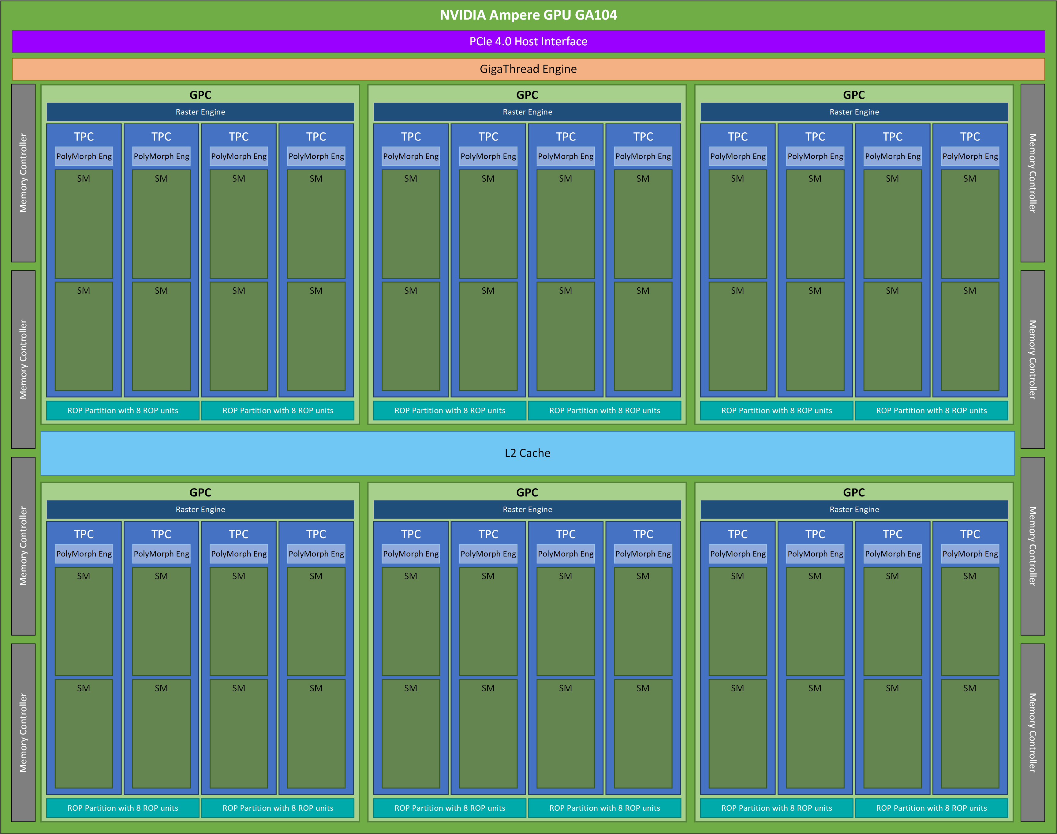 NVIDIA Ampere GA104 architecture.
source: here
NVIDIA Ampere GA104 architecture.
source: here
There is lot to unpack here, these aspects and grouping is related to computer graphics and can be used via vulkan/opengl. I am just going to give brief description on these part and not go indepth.
Let us have brief functionality of each part:
- Giga-Thread Engine: One of the key feature in modern GPUs is the ability to run several kernels in parallel on the same device. All the blocks from different kernels are first given to top-level scheduler (called the Giga-Thread Engine). It is responsible for dispatching blocks to SMs. This dispatching can be dynamic, takes into account of future loads and asynchronous.
- Memory Controller: Memory controllers contain the logic necessary to read and write to dynamic random-access memory(DRAM), and to provide the critical memory refresh and other functions. It also connects various memory units to the main processor bus system.
- GPU processing cluster (GPC): The Graphics Processing Cluster (GPC) is a dedicated hardware block for computing, rasterization, shading, and texturing. These are terminologies are related to computer graphics. The GPC consist of set of TPC, Raster engine and ROP units.
- Raster Engine: The raster engine converts vector graphics (such as 3D models) into raster images (pixels). This enables SPs to execute on these pixels instead of doing complex conversion task.
- ROP units: Raster Operations Pipelines (ROPs) are responsible for the final stages of pixel processing before the image is displayed on the screen. They perform computation for blending, depth testing, gamma correction etc.
- Texture processing cluster (TPC): TPCs are responsible for executing the core graphic workloads that make up the visual experience we see on our screens. They handle functionality of mapping texture, fragment shading, vertex shading etc and they have computation units needed for this task. They contain polymorph engine and set of SMs.
- Polymorph Engine: I do not know much about it, but the hardware units present here is responsible for vertex shading, geometry and texture processing.
Now let us look into the main part which does the parallel computation, the SMs.
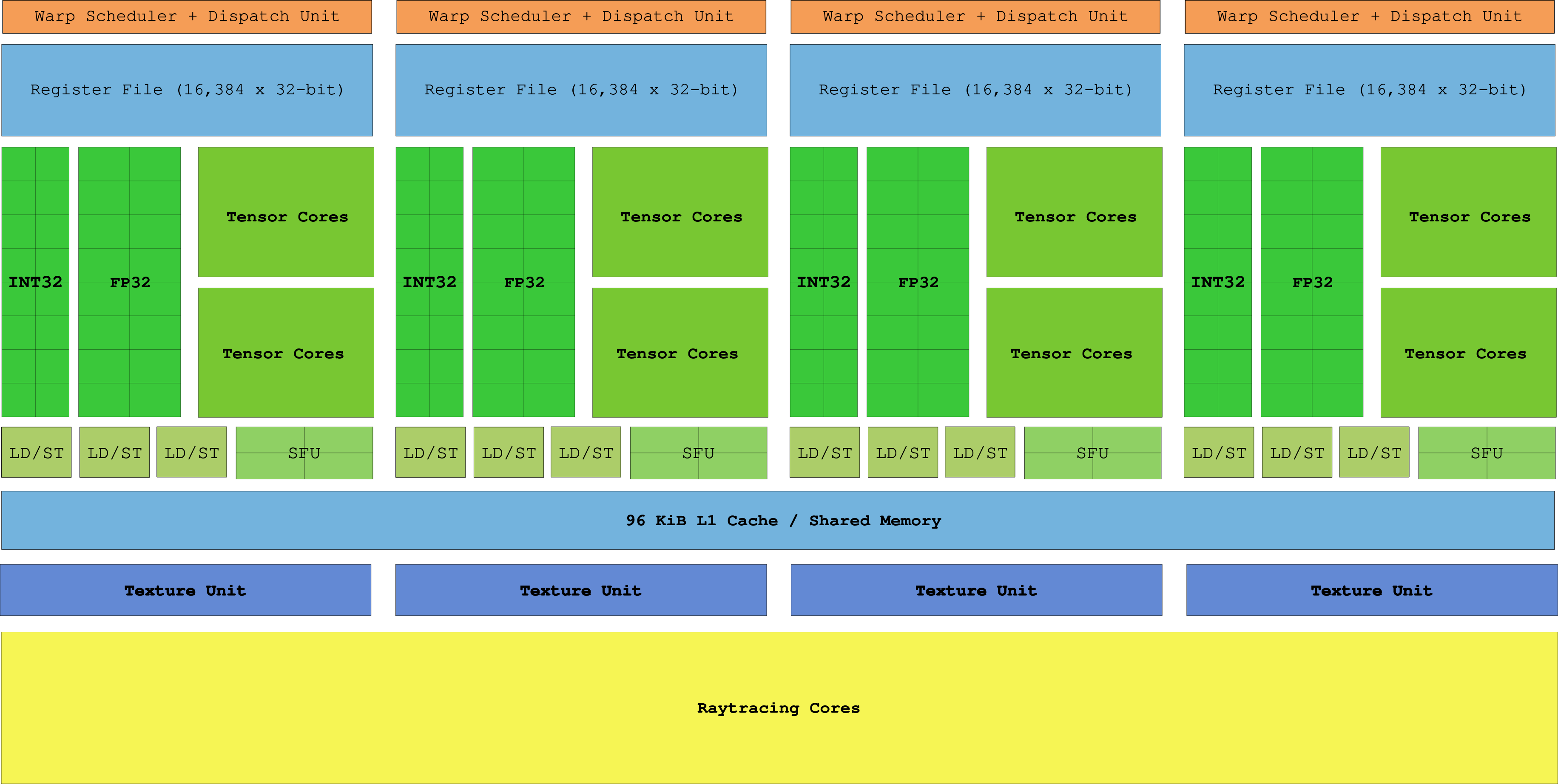 Image of a Streaming Multi-processor (SM)
SM consists of -
- Warp Scheduler: It performs the action of swapping busy warps to save time, this results in latency hiding.
- Dispatch Unit: Dispatch unit assigns warps to the cores, so that everything can run parallel.
- Int32 and FP32 cores: These are the cores that perform simple arithmetic operation.
- Tensor Cores: These are the core, with special units for machine learning related operation. (latest H100, there is even transformer engine).
- LD/ST: These are the load and store units, which access memory needed for the computation.
- SFU: These are special functional unit, that handle computation like erf, sin, cos etc.
- Raytracing cores: These are special hardware units, needed to perform fast but heavy ray-tracing computation.
How does GPU programming maps to Execution on Hardware ? A Story Tale.
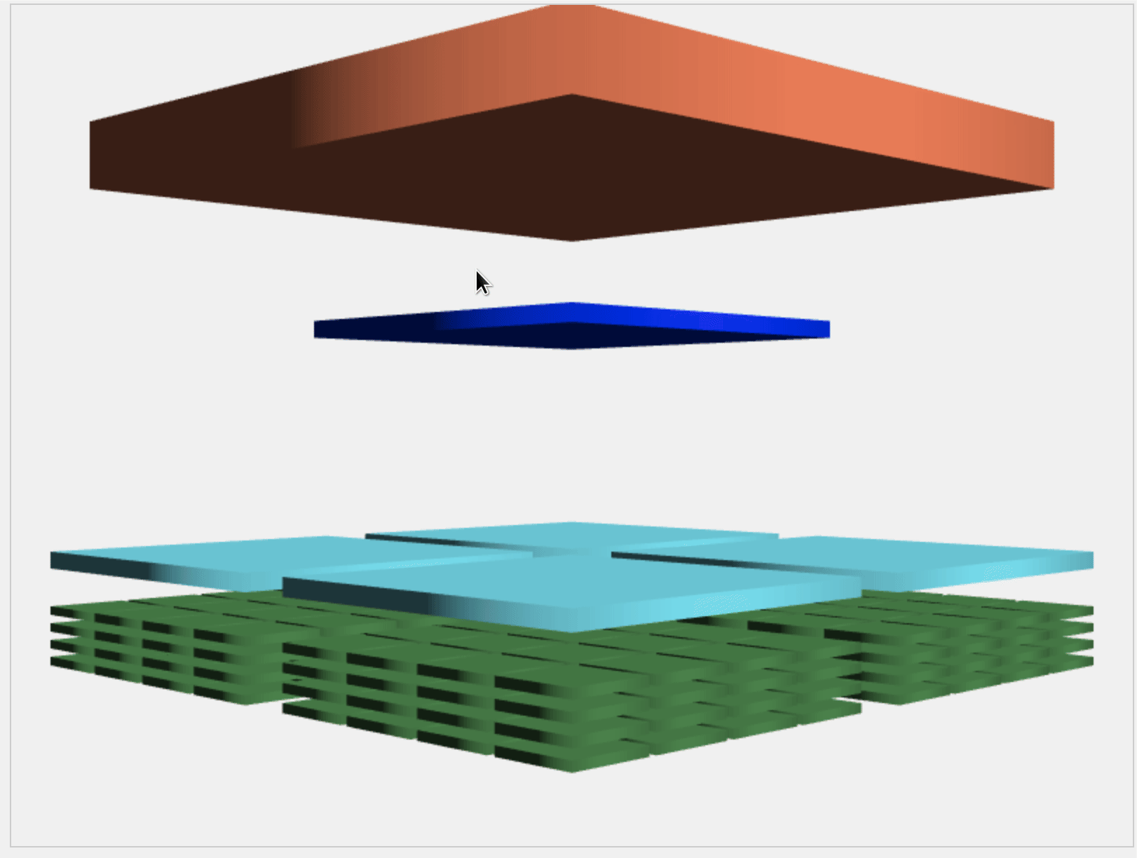
You could check out 3D representation of GPU Hardware and test out few of the Animation made using WebGL. The code is hosted here
There are two aspects to this:
- Data movement via Memory
- How the threads execution on a SIMD system.
Data Movement.
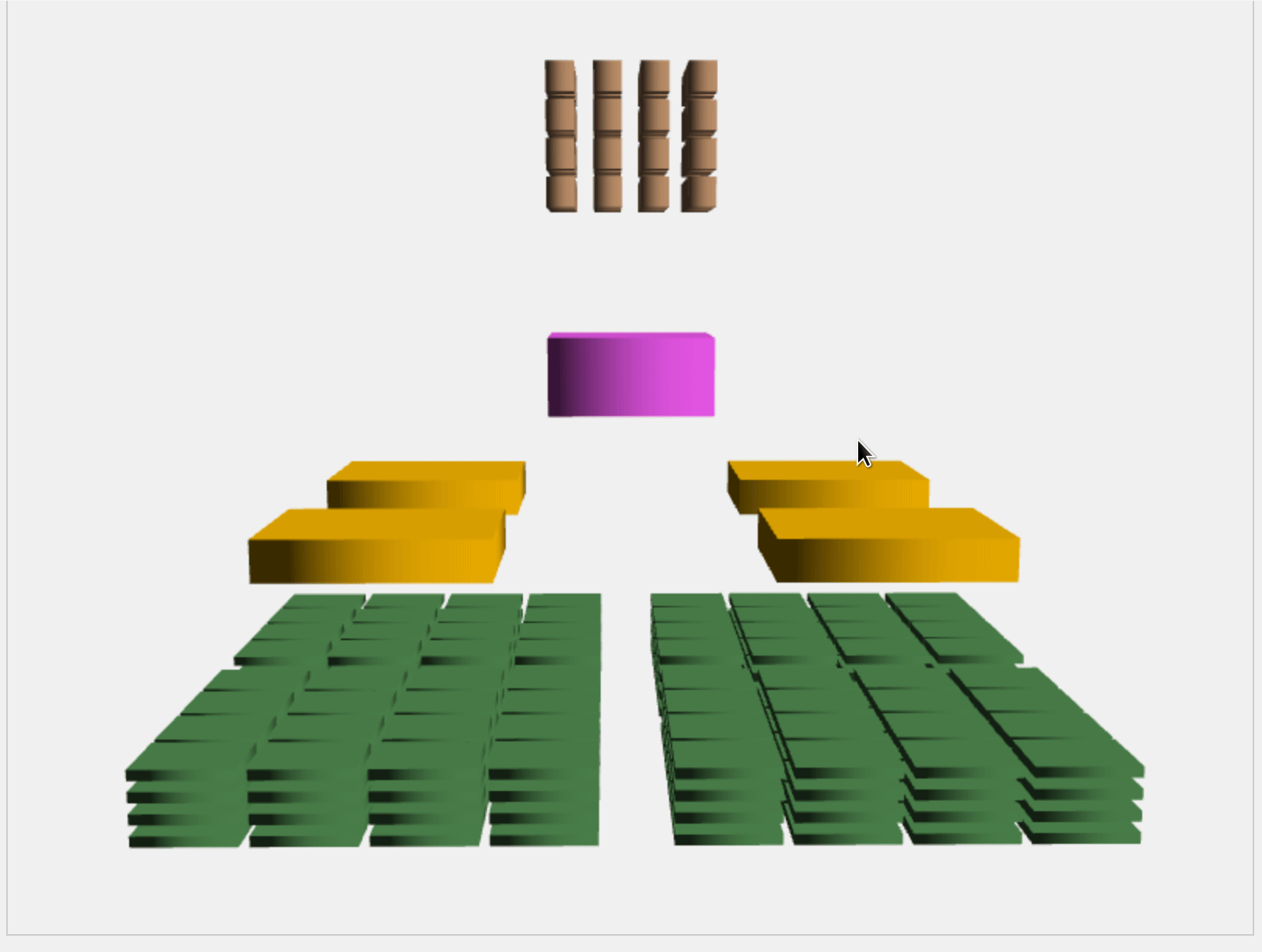
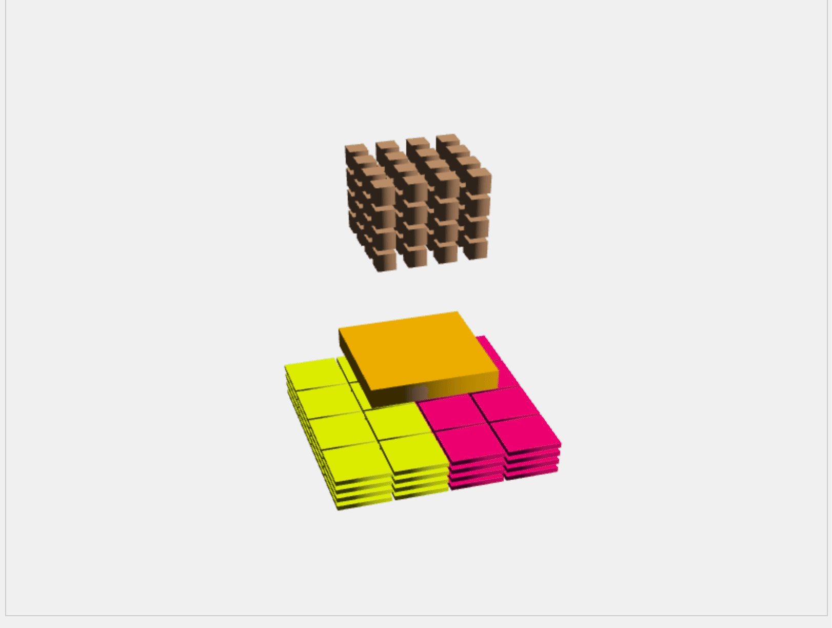
There are 3 Levels of Memory in my view. Global memory, that is the high bandwidth memory in GPU, L2 Cache and Memory exclusive to each SMs (l1 cache, shared memory and registers).
The data that is transfered from host resides in Global memory. This data can be read and written (based on kernel code) by any SPs in any block. As you can see the contention at the global memory is highest and as well as the time taken itself is really high. l1 and l2 cache serves to take advantage of locality and prevent full access via global memory. Less global memory access the better the performance of your GPU program.
 The above animation shows how the memory goes from global memory to l2 cache to l1 cache.
Thread Execution.
There are multiple steps involved here, the Giga thread engine which takes in the blocks from different kernels and sends it to the block scheduler. Then the job of the block scheduler is to assign the blocks to respective SM based on the resources available. The block will be waiting in queue if none of the SM has available resources, including registers, thread slots, shared memory etc. Then, blocks are executed on SMs on different SMs. There is a catch, all the threads in a block are not executed independently on each SMs as having Fetch, decode and execute hardware for each SP can be expensive, so the threads are grouped into warps of 32 threads. Each thread in a warp can implement the same instruction. For further information, read about warp divergence.
 The above animation shows how the block of thread from thread engine goes from global memory to block scheduler to warp scheduler to SPs.
 The above animation describes division of threads to warps and how to goes into each SPs.